Surprise discoveries by Hideo Ohno have led to spintronic technologies that are set to drastically cut the power consumption of memory devices
In 2014, Hideo Ohno and his team at Tohoku University fabricated the smallest spintronic device, with a diameter equivalent to the thickness of a cell membrane - 11 nanometers - and made up of layers the thickness of a sugar molecule - 1 nanometer1. The minuscule technology ran on little power and could store information even without a power source - must-have capabilities for next-generation computer memories and integrated circuits.
It had taken Ohno's team years of searching for the right materials and developing appropriate processing technologies to reach this point. At the nanoscale, says Ohno, even something as simple as measuring a device's diameter can prove challenging - "an electron micrograph of the device looks like Pluto billions of miles away."
But the world of nanoscale spintronics has captivated Ohno for close to three decades now. "The thing that fascinates me most about spintronics is that there has been a constant flow of new discoveries - surprises - that we never could have anticipated," he says. "You flip a stone and you find something unexpected."
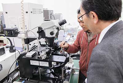
Figure 1:
雷速体育_中国足彩网¥在线直播ers at Hideo Ohno's laboratory in Tohoku University use a specially designed stereomicroscope to examine spintronics components.
Among giants
Conventional electronics involves shunting electrical charge in the form of electrons around circuits. In contrast, the emerging technology of spintronics exploits another property of electrons that has hitherto been ignored - their spin. Harnessing electron spin promises a wealth of benefits, including making devices faster and, more importantly, less power hungry. Ohno's research involves combining the semiconductor technology of conventional electronic devices with magnetic spintronic devices to make efficient, high performance integrated circuits.
He sees his work as following in the footsteps of "two giants" at Tohoku University - Junichi Nishizawa, known in Japan as 'Mr. Semiconductor' for the three most important components underlying optical fiber communication (the PIN junction, laser diode and optical diode), and Shunichi Iwasaki, who invented perpendicular magnetic recording, a technology now universally used in hard drives.
When Ohno first began his research in the late 1980s, semiconductor technologies and spintronics were worlds apart and hard to reconcile. While most integrated circuits are made of semiconducting materials such as silicon or gallium arsenide that are nonmagnetic, mass storage devices are made of magnetic materials with crystal structures that are incompatible with these semiconducting materials. "I wanted to integrate the two by making magnetic semiconductors that could be used in devices," explains Ohno.
By adding the magnetic element manganese to gallium arsenide, Ohno succeeded in 1992 in creating material that was both semiconducting and had the magnetic properties of a permanent magnet known as ferromagnetism2. "Making a material magnetic is different from making a material a magnet," explains Ohno. "But to my surprise, the semiconductor actually became a magnet (a ferromagnet) at low temperatures."
Then, in 2000, he discovered a way to electrically manipulate the ferromagnetic properties of a semiconductor3. And, in 2010, while further exploring the electric-field control of magnetic properties, Ohno's team found a way to magnetize the materials in a perpendicular direction - a finding that led them to develop the smallest spintronic device4. The breakthrough came when the team discovered that they could achieve similar effects on magnetic metals as they could on magnetic semiconductors.
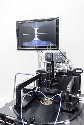
Figure 2:
A system for testing the properties of spintronics components could lead to next-generation computer memories.
Retrieving memory
Ultimately, Ohno hopes to use spintronics to develop memories that retain recorded data even when no power is supplied to them, known as non-volatile memories. Such memories are currently available as flash drives and hard-disk drives, but are yet to be incorporated in integrated circuits - a reality that hits home every time you rue the loss of unsaved data after your computer crashes. Besides making such frustrations a thing of the past, non-volatile spintronics memory based on a type of spintronic device known as magnetic tunnel junctions can also dramatically reduce the power consumption of computing and data storage. Ohno's smallest spintronic device was a magnetic tunnel junction.
"Data centers, such as those established by Amazon, Facebook and Google, are very, very power hungry," explains Ohno. "They generate so much heat that they have to be located near rivers - they're like nuclear power plants."
Much of this power consumption arises because power has to be supplied to volatile memories even when they're not being accessed. "Only about 10 per cent of memory and logic is active at any time; the remaining 90 per cent is awaiting instructions, but you still have to supply it with power," says Ohno. In contrast, as Ohno's memory devices are non-volatile, they do not require power when idle.
Tohoku University offers many advantages to Ohno's research, most notably, its close relationship with industry partners. In particular, Tokyo Electron, the third-largest semiconductor manufacturer in the world, is taking a great interest in the research being done at Tohoku University, evidenced by their donation of a state-of-the-art clean room. "Tohoku University is the only university where you can experiment with 300-millimeter silicon wafers and get results with spintronic components combined with ordinary semiconductor transistors," Ohno says, referring to the industry-standard wafers used by major chip manufacturers.
In February 2015, Tohoku University signed an agreement with Johannes Gutenberg University Mainz to establish a joint-degree program - a first for the university - particularly for PhD researchers in the field of spintronics. "Collaboration works best when you exchange people," says Ohno.
Looking ahead, Ohno is excited about the potential of spintronics and what will be discovered next. The only thing he is absolutely certain of is that there will be more surprises.
-
Sato, H. et al. Properties of magnetic tunnel junctions with a MgO/CoFeB/Ta/CoFeB/MgO recording structure down to junction diameter of 11? nm. Applied Physics Letters 105, 062403 (2014). http://scitation.aip.org/content/aip/journal/apl/105/6/10.1063/1.4892924
-
Ohno, H. Making nonmagnetic semiconductors ferromagnetic. Science 281, 951-956 (1998). https://www.sciencemag.org/content/281/5379/951
-
Ohno, H. et al. Electric-field control of ferromagnetism. Nature 408, 944-946 (2000). http://www.nature.com/nature/journal/v408/n6815/full/408944a0.html
-
Ikeda, S. et al. A perpendicular-anisotropy CoFeB-MgO magnetic tunnel junction. Nature Materials 9, 721-724 (2010). http://www.nature.com/nmat/journal/v9/n9/full/nmat2804.html
Links:

雷速体育_中国足彩网¥在线直播 Institute of Electrical Communication
Center for Spintronics Integrated Systems
WPI Advanced Institute for Materials 雷速体育_中国足彩网¥在线直播,
Center for Innovative Integrated Electronic Systems
Awards
JSAP Compound Semiconductor Electronics Achievement Award -- 2015
IEEE David Sarnoff Award -- 2012
Japan Academy Prize -- 2005
IUPAP Magnetism Prize -- 2003